Solar module innovation is alive and well.
We’ve seen an increase in efficiency of almost 50% from an industry standard 15%, to Longi recently setting a mono PERC record at 22.38%. Just last week, Trina took the “large wafer” concept from the lab to manufacturing line in less than a year. And heterojunction solar modules seek to redefine what is possible.
Researchers at the Massachusetts Institute of Technology and the U.S. Department of Energy’s National Renewable Energy Laboratory have published a paper describing the potential technical and financial outcomes of pushing the solar cell manufacturing industry to thin its solar wafers from today’s industry standard of 160 micrometers (μm) to 50 μm. The paper, Revisiting thin silicon for photovoltaics: a technoeconomic perspective, also gives guidance on the various technologies that’d need to advance to enable this reality.
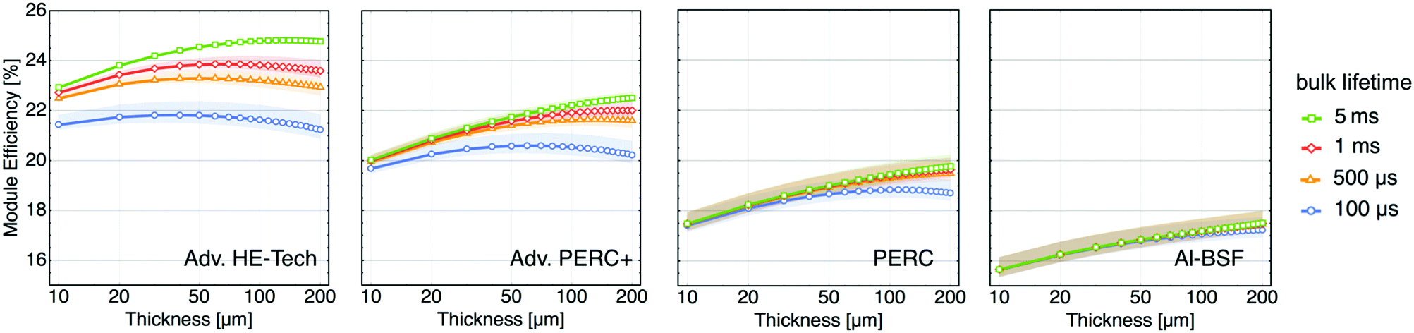
The first step the researchers took was revisiting an old idea — how thin is too thin when it comes to cutting solar ingots into solar wafers? Generally speaking, thinning wafers reduces their ability to capture available photons, especially those photons in the near-infrared spectral range. We thought we’d found a sweet spot at 160 μm thick, however these scientists simulated the thicknesses in the above images across multiple modern and future solar wafer types and came to a conclusion that we can do better.
The researchers note when considering the case of “1 ms bulk lifetime,” the efficiency of 50 μm versus 160 μm thicknesses are 101%, 98%, 97%, and 97% from left to right in the above image — using almost 69% less silicon.
In the above images, AL-BSF represent historically standard aluminum back screen wafers, PERC represents the current product’s we’re buying today, while advanced PERC represents products that we can buy at the cutting edge – like REC Group’s Alpha Product, or Trina and Jinko’s TOPcon products. “Adv HE-Tech” represents future heterojunction products, with advanced efficiencies and qualities designed to take advantage of “thin wafers.”
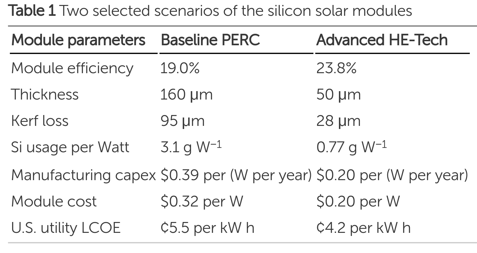
To give you a broader feel for the difference between the current and our cutting-edge future, the above table compares a standard mono PERC wafer at 160 μm versus the advanced heterojunction 50 μm product. Note that kerf loss (wasted silicon ingot between each wafer cut away) goes from 95 μm to 28 μm – which essentially means that almost two entire advanced solar wafers are lost making one modern wafer today.
More notably though, notice how module prices fall from 32¢/W to 20¢/W — a 37.5% fall. Note that it also drops the non-subsidized cost of electricity from these modules, on a power plant level, by 23% – a not trivial number at all. One important thing to note on that 32¢/W price for modern modules – the number is from 2018. We’re currently reaching 24-20¢/W for standard mono PERC modules that are greater than 19% efficiency.
This author speculates that we could adjust the value to consider modern mono PERC at the above mentioned 20 to 24¢/W – and adjust the advanced heterojunction 50 μm product down to a range of 15 to 12.5¢/W for modules.
The report authors looked across the entirety of the solar module manufacturing process and found multiple areas in the process where money could be saved. Looking at 2010 to 2018, the total capex for module production from raw silicon to module declined by 75% from $1.52 to $0.39/watt per year. The advanced heterojunction 50 μm wafers could potentially reduce manufacturing capex by 48% further.
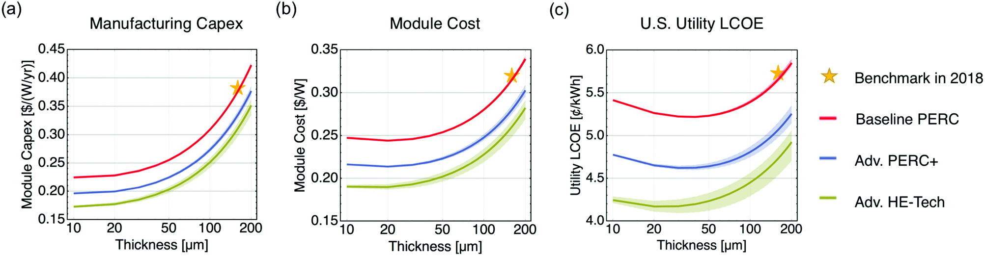
A relationship was found where with every 10 μm thickness reduction, manufacturing capex declines roughly by 1.3¢/W/year, and module cost declines roughly by 0.6¢/W/year. The authors found that thin silicon, regardless of whether using existing, cutting edge, or developing cells can reduce cost of electricity by more than 5% relative to 160 μm wafers. To put it in perspective, the industry has transitioned to PERC to harness the 3% reduction in LCOE.
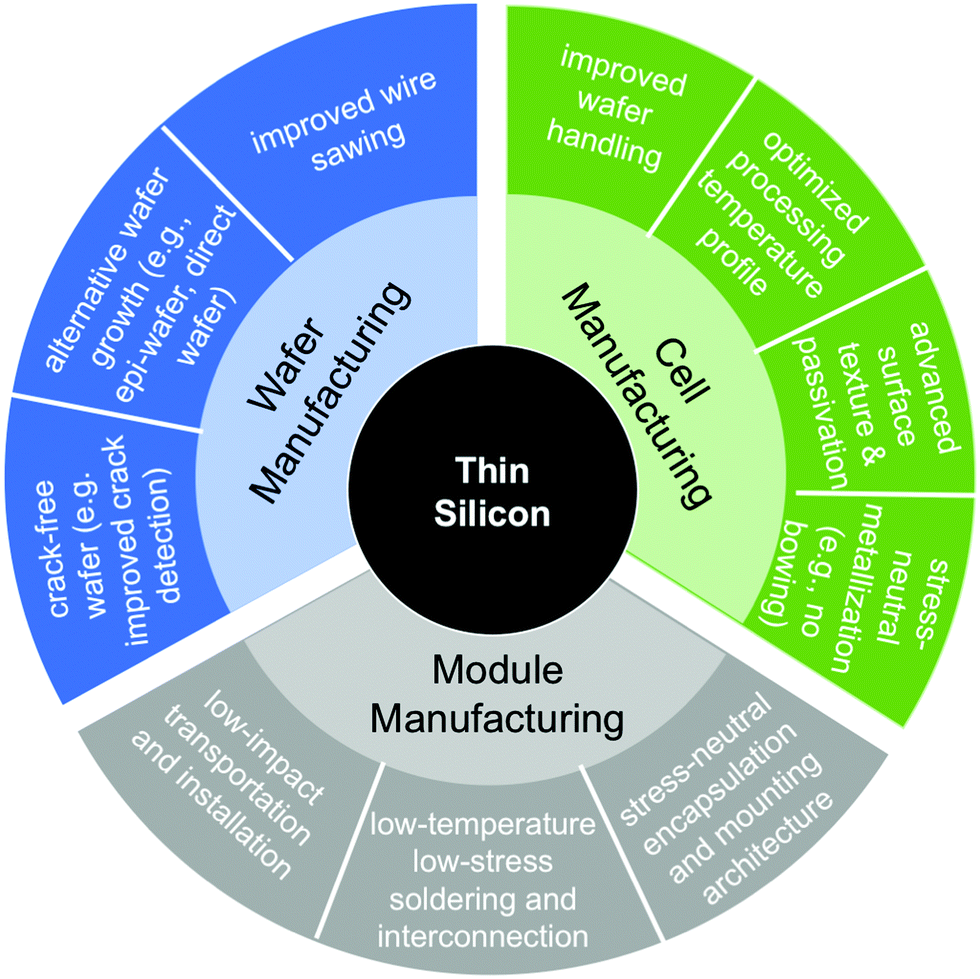
To gain the greatest benefits put forth in this paper, those of the advanced heterojunction solar cell, new solutions must be found in multiple areas as noted in the below chart. For instance, we need to learn how to cut thinner wafers. The current cut is a 255 μm cut, with 95 μm of that being wasted, whereas cutting edge described here is 78 μm — and 70% lesser silicon. Imagine how the silicon ingot manufacturers – feeling massive pricing pressures – might feel if their product suddenly generated three times more than its current value.
This content is protected by copyright and may not be reused. If you want to cooperate with us and would like to reuse some of our content, please contact: editors@pv-magazine.com.


It’s amazing to consider what we can do with technology, isn’t it? But as I read this article, I found myself asking a lot of questions about the long-term consequences of continuing to make product thinner/more fragile. How will these changes affect longevity? If you factor in shorter lifespans due to higher failure/breakage rates, how does that change the economics? Does the lower up-front cost still make it worthwhile? What do we do with this waste stream? What if we build in recycling/decommissioning costs? We need to have a holistic perspective on the implications of continuing to drive costs down and get to a total-cost-of-ownership mentality, not just an up-front-cost mentality.
To change the world more research should be done in almost all institutions.
I am hopefull
We need to first get prices as low as possible and get the longevity and reliability of solar out as far as possibe.
Just throw broken panels to River like Asia does to save money. Lol
A year ago Los Angeles Water and Power Authority, LAWPA, signed contract for 400 MW at an LCOE of $20/mwh= cents 2/kwh over 20 years. How did it get such a low rate? Similar rates have been signed in Portugal, Brazil and Mexico. Where and how much are the subsidies?
The Polysilicon PV technology leaders and the bulk of poly-Si PV manufacturing is in China. Why is the US government bent on helping the competition gain more and more technological advances by funding projects like this at the expense of taxpayer dollars that will questionably help US industry….?
“This author speculates that we could adjust the value to consider modern mono PERC at the above mentioned 20 to 24¢/W – and adjust the advanced heterojunction 50 μm product down to a range of 15 to 12.5¢/W for modules.”
Get the efficiencies up ‘just a little bit more’ and the price points down to this 15 cents/Watt and what’s to stop the typical installation from a 1,000 acre solar PV farm to a 15 to 30kWp roof installation? My concern with 50 um cells is when assembled, does this effect overall resistance to impacts like hail?