The United States of America has decided that solar power is a strategically important technology to develop further and manufacture within our borders.
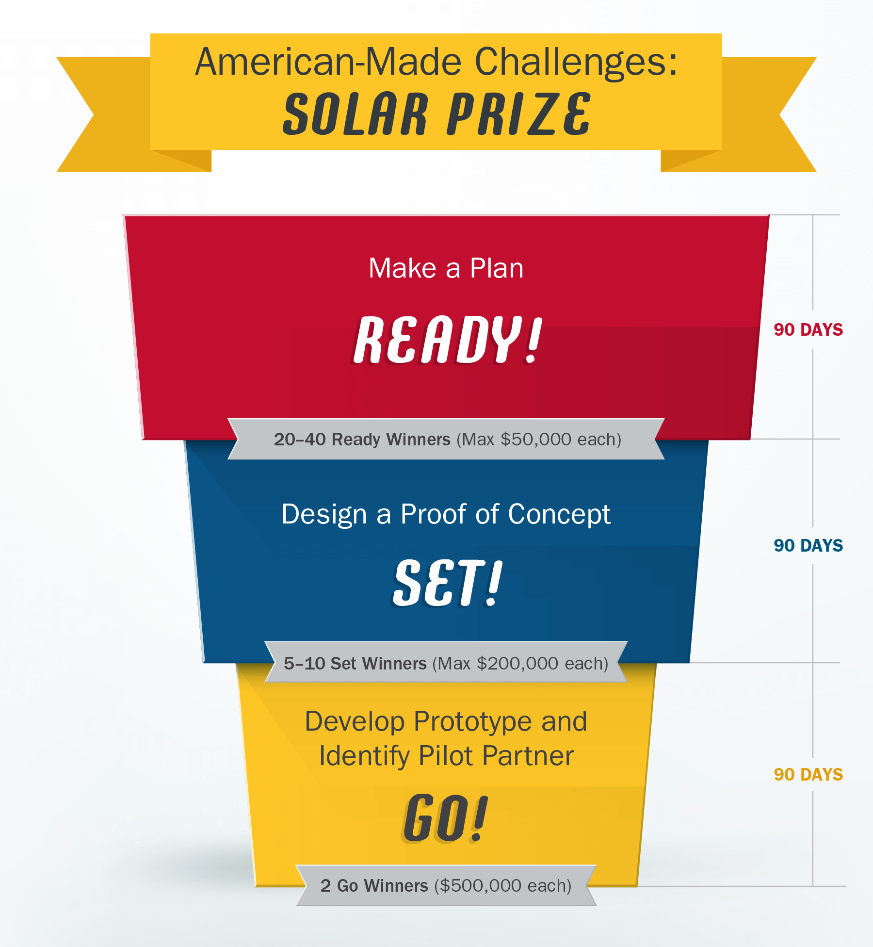 The U.S. Department of Energy’s (DOE) Office of Energy Efficiency & Renewable Energy (EERE) has announced that twenty teams have moved onto the second round of the American-Made Solar Prize. The program aims to connect ideas with the United State’s advanced manufacturing resources.
The teams will work to design a proof of concept over the next three months, then pitch their work to a team of expert judges at a national demonstration day in May. Then, five to ten finalists will compete for two final prizes at a second demonstration day this fall.
High level technical descriptions of the projects can be found on the individual project pages of the twenty teams.
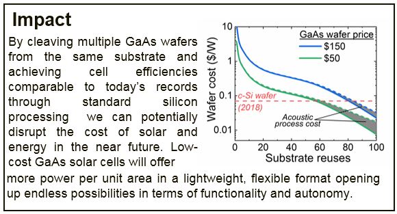
The team from Arizona State University seeks to lower the cost of Gallium Arsenide (GaAs) solar cells by using acoustic cleaving and reusing substrates, and then processing the GaAs solar cells with the same techniques used in standard silicon solar cell processing. The group projects that with substrate reuse and silicon processing, they can get the cost per watt below that of standard silicon solar wafers (see below image).
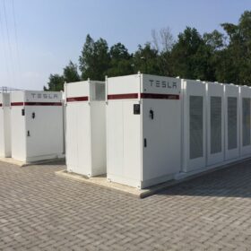
Meanwhile, the BREK Electronics team at University of Colorado Boulder, hopes to deliver a 250 kWac solar string inverter that is lighter, cheaper, with twice the capacity of the largest string inverters (125 kWac), and has a twenty-year lifetime. In the second round filing the group noted that a current challenge is that they have a small company, and the hardware needed to test their designs are generally expensive – and they hope to use the capabilities at the Energy Systems Integration Facility (ESIF) at the National Renewable Energy Lab (NREL). They note that NREL has extensive facilities for solar array simulation and is capable of delivering 1500 VDC at 250 kW with its 1 MW grid simulator, 250 kW bi-directional battery simulator, and 1.5 MW photovoltaic simulator.
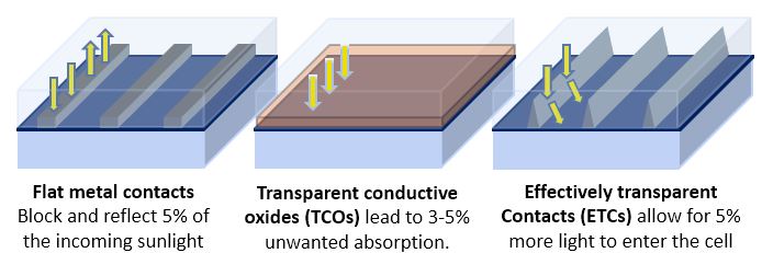
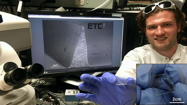
Next, ETC Solar is aiming to commercialize the “world’s highest performing front contact technology for solar cells“, ETC superstrates. As noted in the above image, the fundamental innovation is that the front side contacts are triangular, and the incoming photons sightly glance to the sides and hit the solar cell, versus reflecting backwards. The group projects that their technology can increase a solar cell’s efficiency by 5%. The below image shows a cross section of their front contact at the triangle shape.
And finally, the team from Tandem PV hopes to build a silicon+perovskite tandem solar module, however, instead of attaching the perovskite to the silicon itself, the group hopes to integrate the perovskite film inside of the glass that sits atop the standard solar module. In this second stage of the contest, the group’s proposed goal is to design a functional integrated tandem panel prototype, with the needed electronics.
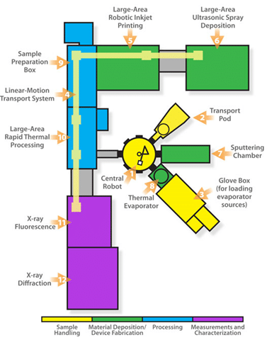
Tandem PV specifically requests the assistance of the Process Development Integration Laboratory (PDIL) at NREL. The Atmospheric Processing Platform (APP) (left image) at the PDIL represents the full complement of equipment to prototype perovskite + silicon tandem modules on a 6” x 6” size. Such tools, if purchased by Tandem PV for private use, would cost approximately $10M.
This program is funded by EERE’s Solar Energy Technologies Office and administered by the DOE’s National Renewable Energy Laboratory (NREL).
This content is protected by copyright and may not be reused. If you want to cooperate with us and would like to reuse some of our content, please contact: editors@pv-magazine.com.


Good luck to them all! I like that NREL has equipment that these teams can use as proof of concept.
Very cool!!! Progress. . . . it’s all about PROGRESS….As a society, As a Country, we must be committed to PROGRESS.
Today, it’s PV Modules. Tomorrow….who knows? Maybe these students will develop their solution on an international scale?
Kudos to the students….Kudos to the University….Kudos to the Administration & Staff involved, thank you….Keep going!!
Regarding Arizona State’s work, I’m curious how acoustic cleaving of substrates works.
Regarding Tandem’s work, Placing the perovskite on the back of the glass cover is a great idea. Separating the persovite, and silicon manufacturing process will make quality control much simpler. I’m curious how electrical contact will be made to the two sides of the Perovskite cell.
Tandem mentions “needed electronics”. Since the different parts of the tandem cell will create different voltages, and will deliver maximum power at different currents, each of them will need it’s own “optimizer” to deliver good performance. Presumably, this could be turned into an advantage by using the electronics on each module as Solar Edge uses it’s optimizers to give a string inverter the ideal DC voltage it needs to create the desired AC voltage, increasing the efficiency of the inverter so much it may be passively cooled, no fans to clean, or perhaps replace. Presumably, the module will have the optimizer outputs in series