A Belgian-Canadian research team claims to have found a way to develop gallium arsenide (GaAs) solar cells at a lower cost while maintaining high power conversion efficiencies.
The scientists said they grew the cell on detachable germanium (Ge) films, which allows the reuse of Ge in other applications, thus reducing production costs. “By ingeniously creating a weak layer between epitaxial layers and a germanium substrate, we unlock the potential for reusing germanium, leading to a significant reduction in both environmental impact and production costs for optoelectronic devices,” Sherbrooke Professor, Maxime Darnon, told pv magazine.
In the paper “High-efficiency GaAs solar cells grown on porous germanium substrate with PEELER technology,” published in RRL Solar, the research team explained that, in order to create this weak layer, it used the so-called PEELER technique, a novel electrochemical porosification technique originally used for silicon wafers.
“The versatility of the PEELER process extends far beyond the realm of traditional solar cell technology,” Darnon said. “From its foundational application in producing high-efficiency solar cells that redefine industry standards to the creation of lightweight and adaptable solar solutions, PEELER opens doors to a myriad of possibilities. Demonstrated with a single-junction solar cell, the concept is applicable to multijunction solar cells. It is perfectly fit for spatial applications where weight and efficiency are paramount. Additionally, the process finds its stride in concentrator photovoltaics, optimizing energy capture in concentrated sunlight environments.”
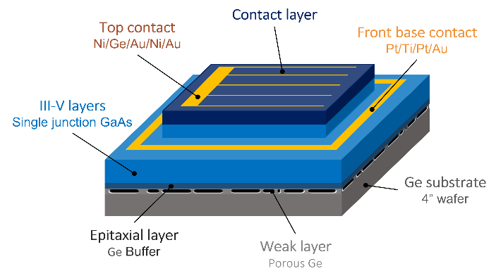
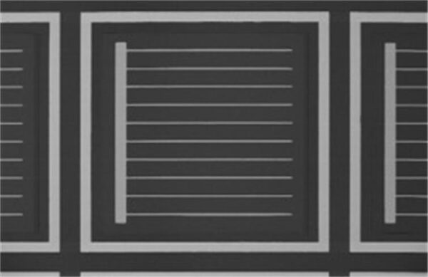
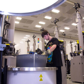
Utilizing metal-organic chemical vapor deposition (MOCVD), the researchers fabricated a 1 mm2 front-contacted GaAs PV device based on a Ge substrate, the weak Ge layer, an epitaxial Ge layer, the GaAs absorber, a top contact made of nickel (Ni), Ge, and gold (Au), and a contact layer.
The champion device built with this architecture achieved a power conversion efficiency of 23.1%, an open-circuit voltage of 1.012 V, a short-circuit current density of 26.28 mA/cm2, and a fill factor of 81.98%.
“The demonstrated performance of single-junction GaAs photovoltaic cells on porosified 100 mm Ge wafers not only matches but surpasses state-of-the-art GaAs solar cells fabricated on detachable substrate, showcasing the transformative potential of growing high-efficiency optoelectronic devices on detachable Ge films,” Darnon stated.
The academics said their experiment also showed the compatibility of the porous structure with the MOCVD growth technique, which they claimed confirmed the industrial potential of the proposed approach.
The research group was formed by scientists from Canada’s Université de Sherbrooke, Canadian energy project developer Saint-Augustin Canada Electric Inc., and Belgian Germanium materials provider Umicore Electro-Optic Materials.
This content is protected by copyright and may not be reused. If you want to cooperate with us and would like to reuse some of our content, please contact: editors@pv-magazine.com.


By submitting this form you agree to pv magazine using your data for the purposes of publishing your comment.
Your personal data will only be disclosed or otherwise transmitted to third parties for the purposes of spam filtering or if this is necessary for technical maintenance of the website. Any other transfer to third parties will not take place unless this is justified on the basis of applicable data protection regulations or if pv magazine is legally obliged to do so.
You may revoke this consent at any time with effect for the future, in which case your personal data will be deleted immediately. Otherwise, your data will be deleted if pv magazine has processed your request or the purpose of data storage is fulfilled.
Further information on data privacy can be found in our Data Protection Policy.