A group of researchers in Germany has developed a comprehensive optoelectrical simulation model for triple-junction solar cells based on subcells relying on perovskite, perovskite, and crystalline silicon, respectively.
The model is intended to define an efficiency roadmap for improving the optical properties of these solar cells within realistic boundary conditions. “The roadmap includes the adaption of the perovskite absorber thicknesses, modifying bandgaps, employing a fully textured cell, and optimizing the thicknesses of the interlayers between the absorbers,” the scientists explained. “We calculate the respective photocurrent of each step and compare it against the theoretical limit.”
For their modeling, the academics chose the Sentaurus TCAD, which is a multidimensional simulator capable of simulating the electrical, thermal, and optical characteristics of silicon-based devices. It is also used to simulate the optoelectronic characteristics of semiconductor devices, such as image sensors and PV cells.
“This tool has already demonstrated its capability in accurately describing the optical properties of perovskite tandem solar cells,” they said, referring to previous, similar research they conducted on perovskite-silicon tandem cells. In this work, they concluded that the practical power conversion efficiency potential of perovskite-silicon tandem devices may reach up to 39.5%.
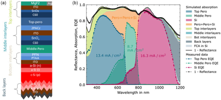
In their most recent work, the researchers initially assumed the triple junction cell to be based on a bottom silicon heterojunction cell with an indium tin oxide (ITO) layer and a silver (Ag) metal contact, a middle perovskite cell with an energy bandgap of 1.57 eV, and a top perovskite cell with a bandgap of 1.84 eV.
In the optimization process, their efforts were directed to increase the photocurrent of all three cells. They initially varied the thicknesses of the three absorbers and then they adjusted the perovskites bandgaps. Moreover, they applied a textured front side to mitigate reflection losses and used thinner interlayers. “Adapting the perovskite absorber thicknesses is rather simple but has the potential to achieve current matching between the top and middle cell,” the group emphasized. “This way the current can be improved significantly.”
The scientists also gauged the thickness of the anti-reflective coating based on magnesium fluoride (MgF2) by reducing its thickness from 130 nm to 90 nm. They also initially increased the thickness of the middle cell’s perovskite absorber, which they said reduces photon absorption in the silicon subcell, but offers improved absorption in the top and middle devices, thus increasing photocurrent at the triple-junction cell level.
The simulation showed that the best cell configuration may potentially achieve a power conversion efficiency of 44.3%, an open-circuit voltage of 3480 mV, a short-circuit density of 14.1 mA cm−2, and a fill factor of 90.1%. This was achieved with a middle perovskite cell with an energy bandgap of 1.46 eV and a top perovskite cell with a bandgap of 1.97 eV.
“On the other hand, we showed that the range of the top-cell bandgap could be chosen between 1.8 and 2.0 eV, depending on the top cell thickness varying between 200 and 800 nm, respectively, for which each a bandgap/thickness tuple exists to achieve global current matching,” the scientists stressed. “Nevertheless, we raised awareness for choosing thicker perovskite layers with higher bandgap to unleash the full open-circuit voltage potential of the top cell.”
Their findings are available in the paper “Optoelectrical Modeling of Perovskite/Perovskite/Silicon Triple-Junction Solar Cells: Toward the Practical Efficiency Potential,” which was recently published in RRL Solar. The research team was formed by scientists from the University of Freiburg and Fraunhofer Institute for Solar Energy Systems (Fraunhofer ISE).
This content is protected by copyright and may not be reused. If you want to cooperate with us and would like to reuse some of our content, please contact: editors@pv-magazine.com.


The information is promising for future solar technology advancement