At the National Renewable Energy (NREL) lab in Colorado, researchers have found that sound waves could bring costs down in manufacturing solar cells traditionally used in space-based applications, making them affordable enough for use here on Earth.
Researchers used sound waves in a new process called acoustic spalling, which was developed at Arizona State University and is now being commercialized by Crystal Sonic Inc, a company located in Phoenix. The study found that the process, also called sonic liftoff, could reduce the costs of manufacturing this type of highly efficient solar cells.
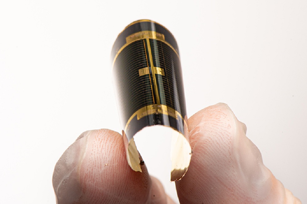
III-V solar cells offer the highest solar PV conversion efficiencies of any technology, according to the NREL researchers. The problem is that the cost of manufacturing has been high, making them too expensive for use in anything but space-based applications.
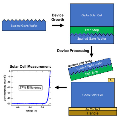
The III-V solar cells are named for the elements used in their manufacture that come from the III and V groups of the periodic table. About one-third of the cost of the cell comes from the single-crystalline substrate on which is it grown, and the researchers found that acoustic coupling can potentially enable the substrate to be reused. The researchers studied the vapor growth of gallium arsenide (GaAs) solar cells on previously “spalled” substrates in order to understand how it affects subsequent device growth and performance.
“This is super promising for the substrate reuse,” said Kevin Schulte, a scientist in NREL’s High-Efficiency Crystalline PV group and the lead author of the journal article detailing the success of acoustic spalling. “This alone will not make III-V solar cells cost-effective, but as part of this portfolio of research, we’re trying address cost from multiple different angles.”
The researchers describe their work in, “GaAs solar cells grown on acoustically spalled substrates with 27% efficiency,” published in the journal Joule.
The technique using sound waves could replace the existing process, which uses a sacrificial etch layer that allows a cell to be lifted off a GaAs substrate so the substrate can be reused. The drawbacks, however, are that it’s a lengthy process and it leaves behind a residue that adds an expensive polishing step.
Source: NREL
Spalling, on the other hand, takes seconds. It works by creating a controlled fracture within the substrate nearly parallel to its surface, and the fracture allows the cell to be easily removed, revealing a new, contaminant-free surface from within the substrate that does not require polishing. Acoustic spalling uses sound waves to control the fracture, suppress the formation of facets and improve the flatness of the substrate.
“The surface is less corrugated,” Schulte said, “so when you grow a new device on it, it’s possible to achieve a high efficiency with relatively minimal, or potentially no, surface repreparation.”
The researchers indicated that additional research is needed to determine how many times the substrate can be reused after being subjected to acoustic spalling. The researchers were able to make a cell on a previously spalled substrate with an NREL-certified efficiency of 26.9%.
“I don’t think there’s any difference in that performance compared to what efficiency we could get on a brand-new substrate,” Schulte said.
This content is protected by copyright and may not be reused. If you want to cooperate with us and would like to reuse some of our content, please contact: editors@pv-magazine.com.


It’s a shame for authors of this research to claim acoustic sound is their method. This method already introduced by researchers from Shanghai Jiao tong university and the group focused on this method for eight years. This also reflects reviewers of joule journals were not qualified to review.