As other kerfless wafer manufacturers disappeared from the market, 1366 Technologies was warned that it, too, would eventually suffer the same fate. And yet still, the company persisted.
Their confidence and commitment continue to pay off – for itself, its partner Hanwha Q Cells and the industry, which continues its search for innovations in the production process.
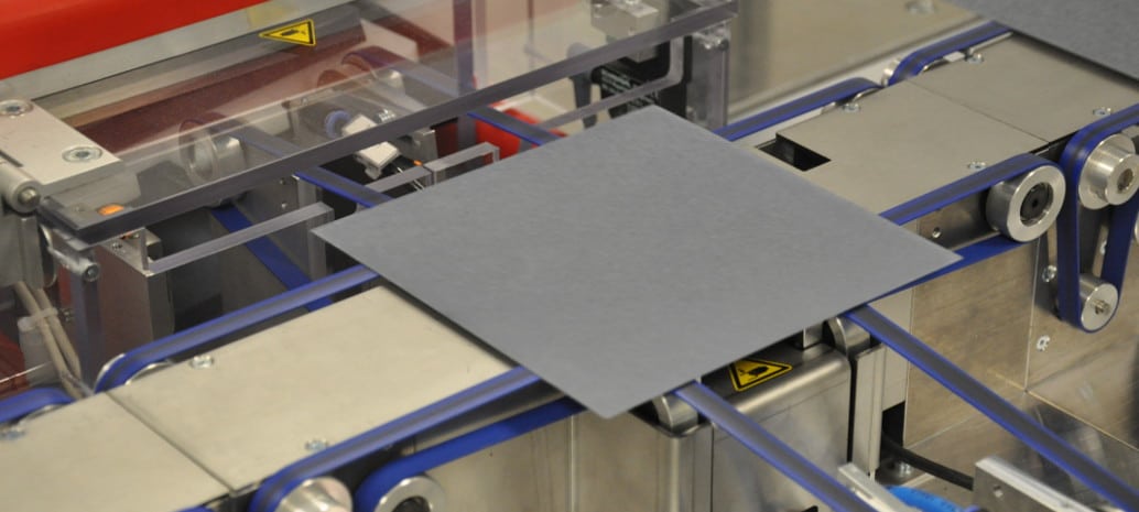
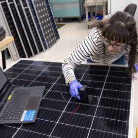
The most recent 1366 achievement a 20.3% efficient champion cell based on its Direct Wafer and Passivated Emitter Rear Contact (PERC) technology, which puts it among the higher numbers in the industry. Fraunhofer ISE CalLab confirmed with independent tests, as well as a 20.1% average efficiency for PERC cells produced on a pilot line with partner Hanwha Q Cells.
“Our strategic partnership with Hanwha Q CELLS is paving the way for a solar future where high-efficiency cells are realized at a substantially lower cost,” said Frank van Mierlo, CEO of 1366 Technologies. “Working at the melt level, rather than an ingot, means you can play with the make-up of the wafer as it is being formed.”
Van Mierlo also stated that the company is “rapidly closing in on” a 21% efficient cell, in collaboration with Hanwha’s Q.ANTUM cell technology. This is on top of the efficiency advantages of 1366’s Direct Wafer process, which does not produce the saw waste that other processes do.
“The simple fact is sawing ingots – whether cast multi or pulled mono – is wasteful and energy intensive,” van Mierlo added. It’s an old process for a modern industry.”
1366 produced the wafers at its headquarters Bedford, Massachusetts, and Hanwha finished the cell fabrication at Hanwha Q CELLS’ Center for Technology, Innovation, and Quality in Thalheim, Germany. Only five months ago, 1366 had reached a new efficiency record of 19.9% with its technology and reported its first deployment in a 500 MW commercial project in Japan.
There is still no word on when 1366’s new commercial-scale facility in Upstate New York will be mass-producing wafers. The company notes that it is waiting on a U.S. Department of Energy-backed loan to fund the factory, and but that while waiting, it has “accelerated our plans to build factories in locations around the world and are currently in active positive discussions to do just that”.
This content is protected by copyright and may not be reused. If you want to cooperate with us and would like to reuse some of our content, please contact: editors@pv-magazine.com.


By submitting this form you agree to pv magazine using your data for the purposes of publishing your comment.
Your personal data will only be disclosed or otherwise transmitted to third parties for the purposes of spam filtering or if this is necessary for technical maintenance of the website. Any other transfer to third parties will not take place unless this is justified on the basis of applicable data protection regulations or if pv magazine is legally obliged to do so.
You may revoke this consent at any time with effect for the future, in which case your personal data will be deleted immediately. Otherwise, your data will be deleted if pv magazine has processed your request or the purpose of data storage is fulfilled.
Further information on data privacy can be found in our Data Protection Policy.