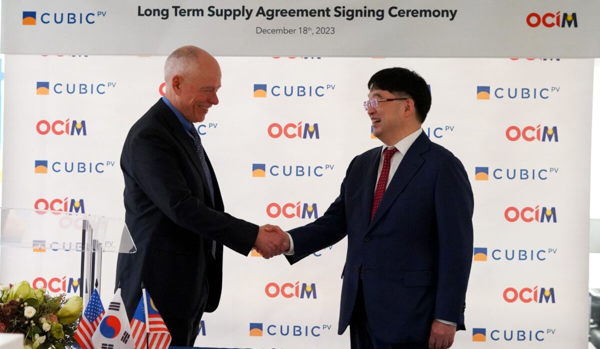
Silicon solar wafer manufacturer CubicPV and silicon producer OCIM announced an eight-year supply agreement in which Cubic becomes OCIM’s first U.S. customer for its low-carbon, U.S. compliant silicon.
The contract, which Cubic reports is valued at approximately $1 billion, establishes a commitment for an annual supply volume by OCIM, providing Cubic with the polysilicon it needs in order to begin manufacturing at its U.S. plant
One year ago CubicPV announced plans to establish 10 GW of conventional mono wafer capacity in the United States. Driven by incentives in the Inflation Reduction Act, Cubic reports that the wafers produced by the new facility could fill a void in the domestic supply chain as well as create 1,500 new direct jobs.
The silicon supply from OCIM reportedly satisfies U.S. law, helping CubicPV to produce domestic silicon wafers to serve the U.S. solar industry. Cubic reports that during the past six months it has produced “significant wafer volumes” using OCIM silicon, which meet or exceed customer specifications.
“This agreement with one of the world’s foremost leaders in polysilicon production is testament to our manufacturing capabilities and the progress against our U.S. manufacturing plans,” said Frank van Mierlo, CEO, CubicPV. “OCIM’s high-quality, U.S. compliant silicon is in extremely high demand, and we are fortunate to lock-in our supply with a trusted supplier,”
Under the terms of the agreement, OCIM will begin to provide silicon in 2025 from its manufacturing facility, which OCIM reports is powered by clean, hydroelectricity.
CubicPV was formed from the merger of Hunt Perovskite Technologies and 1366 Technologies, a company that was founded in 2008 and headquartered in Bedford, Mass. 1366 Technologies was known for its direct wafer technology, which forms wafers directly, using molten silicon, instead of silicon ingots sawn into wafers. The advantage is less loss because it uses a kerfless wafer production that does not require silicon ingots to be sawn into wafers, a time-consuming process that wastes material as silicon dust. Instead, 1366’s technology forms wafers directly, using molten silicon.
CubicPV intends to produce M10 and G12 n-type wafers in its facility in the U.S. The exact location has not yet been disclosed.
This content is protected by copyright and may not be reused. If you want to cooperate with us and would like to reuse some of our content, please contact: editors@pv-magazine.com.






By submitting this form you agree to pv magazine using your data for the purposes of publishing your comment.
Your personal data will only be disclosed or otherwise transmitted to third parties for the purposes of spam filtering or if this is necessary for technical maintenance of the website. Any other transfer to third parties will not take place unless this is justified on the basis of applicable data protection regulations or if pv magazine is legally obliged to do so.
You may revoke this consent at any time with effect for the future, in which case your personal data will be deleted immediately. Otherwise, your data will be deleted if pv magazine has processed your request or the purpose of data storage is fulfilled.
Further information on data privacy can be found in our Data Protection Policy.