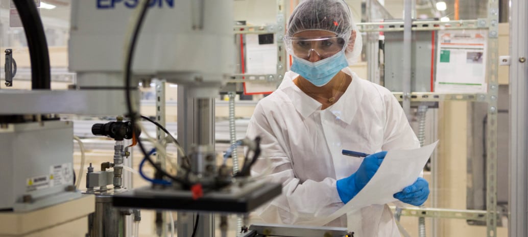
Seven solar manufacturing start-up firms have each received $1 million to develop a “robust prototype” that they could use as a calling card in seeking private investment.
The manufacturing processes the firms are pursuing include two thin-film technologies, silicon wafer splitting, improved metal paste, solar glass coating, a household breaker panel with inverter, and a field factory.
The grants are among 75 grants totaling $128 million that the U.S. Department of Energy’s Solar Energy Technologies Office (SETO) has awarded, toward a long-term goal of reducing costs to 3 cents per kWh for utility-scale PV, 4 cents for commercial/industrial PV, and 5 cents for residential PV.
Twenty-one grants awarded for PV research and development are also covered in this story; SETO also made grants for balance-of-systems, systems integration, and concentrating solar.
Innovations in manufacturing
The seven entrepreneur-stage manufacturing companies are located in Washington, California, Arizona, New Mexico, and Michigan. To earn a DOE grant, each firm provided a cost-share ranging from $300,000 to $1 million.
As a means to manufacture perovskite cells, Bluedot Photonics is developing single-source vapor deposition hardware in which a powder is converted directly to vapor and coated onto a substrate, the base of a solar cell.
To speed production of silicon carbide wafers for power electronics, Halo Industries will deliver a technology that mechanically fractures wafers off blocks of silicon carbide without wasting material.
Osazda Energy will develop an improved screen-printable metal paste, which strengthens metal connections in a solar cell, and test it in concert with Sandia National Laboratories.
A tool that takes transparent conductive oxide, and rapidly deposits it onto heterojunction silicon with intrinsic thin layer (HIT) solar cells, will be developed by Scion Plasma.
Hardware for solar-plus-storage systems, that integrates a hybrid inverter into a breaker panel, will be developed by Span.io.
Swift Coat will make and scale anti-reflective and anti-soiling coatings for solar glass, deposited onto the glass by spraying dry nanoparticles, and test coated glass in concert with the National Renewable Energy Laboratory.
Terabase Energy will create a field factory that delivers PV power plants and reduces soft costs.
PV research and development
SETO’s PV research and development grants support projects that will help reduce PV costs, increase PV performance, and improve reliability.
SETO made seven grants for PV research collaborations, ranging from $1.8 million to $4.5 million, with each grant having a cost-share requirement. Universities are leading four of the collaborations:
- Proving the viability of a sonic wafering process to remove gallium arsenide solar cells from the top surface of a thick wafer to reuse III-V substrates (materials from groups III and V of the periodic table): $2.5 million to Arizona State University
- Developing a test foundry that U.S. companies may use to prove the viability of new PV technologies, focusing on post-passivated emitter rear contact cell and module technologies: $1.8 million to Arizona State University
- Identifying the best materials to use to make high-quality passivated rear contacts for thin-film cadmium-telluride (CdTe) solar cells: $3.5 million to Colorado State University
- Using machine learning and developing algorithms to automate maintenance decisions at utility-scale PV plants: $2 million to Electric Power Research Institute
- Developing new methods for roll-to-roll printing of bifacial thin-film PV modules: $4 million to Energy Materials Corporation
- Improving a floating-silicon method for producing continuous thin silicon ribbons that are then cut into wafers: $2.5 million to Leading Edge Crystal Technologies
- Developing high-efficiency thin-film perovskite mini-modules and investigating deposition techniques: $4.5 million to the University of Toledo.
SETO also made 14 grants of $200,000, each with a cost-share of $50,000, for small innovative research and development projects that are “intended to provide a foothold for new technologies or areas of study”:
- Module lamination research
- Polymeric hole transport materials for perovskite
- Research into light- and elevated temperature-induced degradation of p-type passivated emitter rear contact (PERC) silicon PV cells
- Tools and methods to measure charge carrier movement in copper indium gallium selenide (CIGS) PV cells
- PV plant designs to enable dispatchable solar
- Co-locating PV and pasture-raised rabbits
- Sealants to reduce lead leakage from broken perovskite modules
- Using artificial intelligence in PV system inverters to provide dispatchable power
- Research on causes of PV cell defects
- Lower-cost printing of silver contacts on silicon PV cells
- Research into reusing the base (substrate) of the solar cell
- Developing and researching a CdTe PERC solar cell
- Research into perovskite PV cell degradation
- Research into producing pure silicon from quartzite.
This content is protected by copyright and may not be reused. If you want to cooperate with us and would like to reuse some of our content, please contact: editors@pv-magazine.com.


Yes, we greatly need research and development to improve efficiency, that is the key to everything. A more efficient module will allow fewer modules, less equipment,less labor etc.
From the Colorado School of Mines: “Project Summary: This project will develop hole transport materials—layers in a solar cell that collect current—using organic materials called polymers that will give thin-film perovskite solar cells, including tandem cells, efficiencies greater than 30% and lifetimes of more than 25 years. Polymers cost less than materials currently used for this purpose, and they will allow the team to manipulate their material properties to achieve greater compatibility with other layers of the device.”
Polymers have been used for years in solar PV panels and it always has come down to yellowing and cracking causing contact and cell sealing problems after several years in Desert conditions. Being able to fix this would be the next big thing in solar PV technology.
University of Central Florida: “Project Summary: This project will enable the printing of silver contacts on silicon solar cells with very little thermal energy use, through a scalable technology called a nanoparticle electrospray laser deposition (NELD). NELD will deposit silver microdroplets on the base of a silicon solar cell, then fuse the nanoparticles together with a laser, a process known as sintering. This project will lower costs and improve cell performance.”
NELD could also be a way to ‘sinter’ different band gap cell technologies together to make binary or trinary solar PV cells. Low energy process needs some more explanation to determine how much less energy is required for the final product. Would it be possible to get to a 40% effective solar insolence harvest? With that kind of efficiency over a 25 to 30 year life product one could see manufacturing using this technology using solar PV and energy storage. Getting rid of overhead creates the ‘tolerant’ manufacturing process. Adding AI to a plant’s operation mix may make an almost autonomous manufacturing facility.