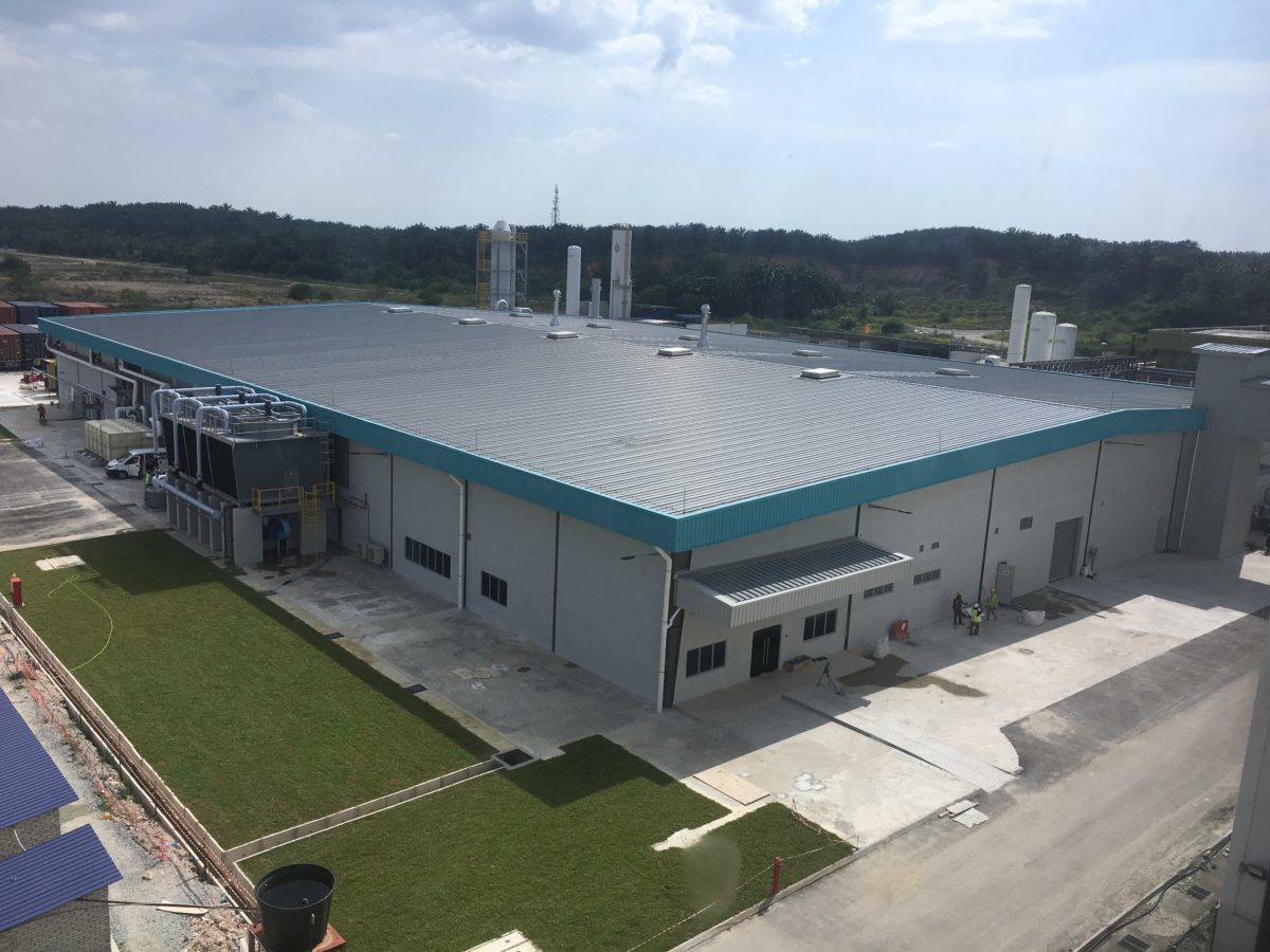
U.S. based wafer maker 1366 Technologies and Hanwha Q Cells’ Malaysian unit have announced construction of their wafer manufacturing facility in Cyberjaya, in the Sepang district of Selangor, is close to completion.
The Direct Wafer Factory, the U.S. company said, was built near Hanwha’s existing cell and module factory in Malaysia to facilitate direct wafer delivery to the Korean manufacturer, which has a 700 MW supply agreement with strategic partner 1366 Technologies.
“The Direct Wafer Factory is expected to ramp no later than Q3 2019 and – provided that the initial footprint meets key performance criteria – has the potential to become the cornerstone for a multi-gigatt scale production facility,” the U.S. wafer maker announced.
Hanwha Q Cells chief technology officer Ji Weon Jeong said: “In line with this commitment to customer value, Direct Wafer technology will innovate the manufacturing process and, as a result, the quality of the products manufactured.”
The promise of kerfless wafering
In March, 1366 Technologies said it was abandoning plans to build a wafer manufacturing facility in New York and would construct its first commercial-scale wafer factory at an undisclosed overseas location. As part of the change in strategy, the company had withdrawn from the loan guarantee process of the U.S. Department of Energy without having received funds.
Promising to bring kerfless wafer technology to mass production, 1366 Technologies’ Direct Wafer technique has long held big hopes for the industry. The company currently operates a demonstration facility in Bedford, Massachusetts, where most of its technological developments were achieved. One such was the 20.3% cell efficiency reached in August 2017 in a Q Cells Q.ANTUM cell, incorporating passivated emitter rear contact (PERC) technology and 1366 Technologies wafers. That record, 1366 Technologies said at the time, was achieved on a pilot line using standard processes seen in mass production.
Price reduction
The Bedford-based company said the new manufacturing facility could lead to the production of wafers for less than $0.20 per piece, and its Direct Wafer process enables the production of thinner 3D wafers by reducing the amount of silicon used to less than 1.5 g/W without compromising quality. The company said its production process has other advantages, such as a high-purity growth environment, better microstructure and the ability to grade doping agents across the wafer.
Kerfless wafer production does not require silicon ingots to be sawn into wafers, a time-consuming process which wastes up to 44% of the material which becomes silicon dust. 1366’s kerfless technology forms wafers directly, using molten silicon.
1366 is also partnering with German polysilicon manufacturer Wacker Chemie.
This content is protected by copyright and may not be reused. If you want to cooperate with us and would like to reuse some of our content, please contact: editors@pv-magazine.com.


By submitting this form you agree to pv magazine using your data for the purposes of publishing your comment.
Your personal data will only be disclosed or otherwise transmitted to third parties for the purposes of spam filtering or if this is necessary for technical maintenance of the website. Any other transfer to third parties will not take place unless this is justified on the basis of applicable data protection regulations or if pv magazine is legally obliged to do so.
You may revoke this consent at any time with effect for the future, in which case your personal data will be deleted immediately. Otherwise, your data will be deleted if pv magazine has processed your request or the purpose of data storage is fulfilled.
Further information on data privacy can be found in our Data Protection Policy.