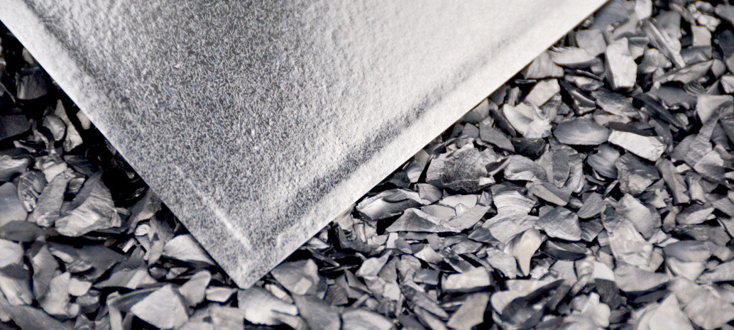
While a number of start-ups have produced kerfless silicon wafers – wafers fabricated without the messy, heavy process of slicing ingots – none has achieved the level of commercialization that 1366 Technologies has.
Today the kerfless wafer maker announced a new technological feat, unveiling thin 100-120 micron wafers with a border of the standard 180-200 micron thickness, as the world’s first “three-dimensional” wafer product. 1366 says that this allows for reduction of silicon use to around 1.5 grams per watt without compromising strength, performance or durability.
1366 notes that a 3-D design is impossible with conventional crystalline silicon technology. And while with conventional wire sawing techniques wafers thinner than the standard 180-200 microns can be produced, such wafers are not as strong and have a tendency to break during the chemical and industrial processes which turn them into PV cells and modules.
The wafer maker says that is ready to begin producing 3-D wafers as soon as the cell industry is ready for them, which alludes to the possibility that changes to cell and module processes may be needed to accommodate the new wafers.
1366 is currently building the world’s first commercial-scale kerfless wafer factory in Upstate New York, and in May announced that it had reached $32.5 million in its series C round, some of which will be used to build the facility. The company has additionally secured a contract with Hanwha Q cells to supply 700 MW of its Direct Wafers when the factory comes online.
This content is protected by copyright and may not be reused. If you want to cooperate with us and would like to reuse some of our content, please contact: editors@pv-magazine.com.


By submitting this form you agree to pv magazine using your data for the purposes of publishing your comment.
Your personal data will only be disclosed or otherwise transmitted to third parties for the purposes of spam filtering or if this is necessary for technical maintenance of the website. Any other transfer to third parties will not take place unless this is justified on the basis of applicable data protection regulations or if pv magazine is legally obliged to do so.
You may revoke this consent at any time with effect for the future, in which case your personal data will be deleted immediately. Otherwise, your data will be deleted if pv magazine has processed your request or the purpose of data storage is fulfilled.
Further information on data privacy can be found in our Data Protection Policy.